August 22, 2023
Smart solutions in semiconductor manufacturing
Semiconductor technology has come a long way since Robert Noyce fabricated his first silicon device: smaller chips, more transistors and incredible performance gains. But as transistor sizes approach atomic scales, there are more concerns about precision and accuracy in the fabrication process than ever before. Moore’s law is a double-edged sword: the more we can do with semiconductors—and the faster we make them—the more challenges we face during fabrication.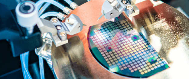
Higher speed, higher risks
Take throughput, for example. If you upgrade from a $1 million machine that tests 100 silicon wafers per hour to one that tests 200, you’ve just doubled your productivity (and lowered your cost of ownership by half). But as throughput increases, so does the risk to accuracy and positioning. Heat becomes an issue as well. The faster your machine goes, the hotter it runs, which can cause thermal expansion because it’s made from metals such as aluminum, steel and silicon alloys—again, a threat to accuracy. And the minuscule scale on which these operations happen exacerbates the issue.
More cables, more issues
There’s also the issue of cabling. Motion systems used in semiconductor capital equipment are burdened with moving bundles of cables that can exceed a mile in length. In particular, the latest encoders on the market provide a treasure trove of data, especially if you mount several of them. A large amount of data is great—the large number of cables you need to transmit it, less so.
Getting smart
These are serious challenges—and they require smart solutions. Smart solutions leverage technology to account for and correct variance in real-time and process data more efficiently, all without adding more cables to already cumbersome systems. This allows manufacturers to review many more wafers at a time without loss of accuracy and to incorporate data from many more sensors without a lot of additional cabling.
A smart solution means you can do more—faster, all while maintaining accuracy, using the same amount of space (or less) and reducing your overall cost of operation. HEIDENHAIN’s solutions make this all possible.
Ever more precise
Underpinning all these challenges is the need for ever-better precision. Extreme Ultraviolet (EUV) lithography, alongside advanced packaging techniques, is pushing the envelope and demanding unprecedented accuracy.
Encoders and motion control systems must be able to sense where the wafer is in three-dimensional space, and its location relative to the optical system that’s being used in fabrication or inspection. When you’re thinking about creating sub 10 nanometer architectures, the room for error is vanishingly small.
HEIDENHAIN’s semiconductor fabrication solutions
HEIDENHAIN solutions maintain accuracy, increase efficiency and reduce the cost of ownership in a few different ways:
Improved machine accuracy through the use of calibration solutions
By mounting our encoders on specially designed substrates, we provide extremely accurate measurement of position compared to traditional encoders. This level of accuracy allows fabricators to calibrate their machines to achieve nanometer accuracy.
More accurate positioning information from encoders
HEIDENHAIN linear encoders can identify the slightest variance in any direction, for example measuring movement perpendicular to the main direction of movement. That information is then incorporated into the motion system, which can adjust its motion trajectory on the fly to compensate. This, again, greatly increases accuracy—and when you can maintain accuracy at higher speeds, you can process more wafers and lower your cost of ownership.
Fewer cables through better interfaces
Using more encoders means more accuracy, but it also means more cables running back to the controls. This can be quite cumbersome, and it means more weight, which in turn downgrades motion system performance. The EnDat 3 interface solves this problem, sending digital data more efficiently over a fast serial interface with a single cable.
Global trends and the push to growing the semiconductor industry’s annual revenue to $1 trillion
Looking beyond the technology itself, the semiconductor industry is in the middle of major changes in how investment is distributed globally. There are very strong fundamental drivers for the need for advanced semiconductor devices, mainly driven by the demand for computation, data storage, data analytics, an increasing emphasis on AI and machine learning applications. Other drivers include the requirements of the Internet of Things (IoT), the connectedness of people and devices around us as well as an increasing need for electronics content in the automotive industry.
Having come through a difficult period of supply constraints, we’re now seeing massive investments in capacity, particularly in the US but also in Europe. While the semiconductor industry was born in the US, the bulk of manufacturing capacity is currently in Asia – but this balance is changing. Governments are getting involved. For example, the CHIPS Act is boosting investment in the US to increase its ability to manufacture semiconductors.
As we look towards the 2030 timeframe, there is a strong expectation that the industry will exceed a trillion dollars, with demand driven by megatrends such as electric vehicles, cloud computing, wireless communications and AI. And a lot of CEOs are now focused on how to support that scaling. For HEIDENHAIN, we work with all the key capital equipment companies supporting the chip manufacturers in this initiative. Our global footprint, the maturity of the company and our philosophy of long-range investment strategies make us very well-positioned to support the challenges of scaling in the supply chain.
The HEIDENHAIN difference
HEIDENHAIN, and our subsidiary ETEL, occupy a unique place within the market. Our products touch on virtually every place in the semiconductor manufacturing process, from front end to back end to assembly. When you look at the machines that make 95% of semiconductor devices worldwide, you’ll find they all include HEIDENHAIN products – take away our equipment, and you can’t make your smartphone.
Our core competence is delivering technology that enables capital equipment companies to achieve the type of accuracy, precision and throughput necessary for any given application within the semiconductor manufacturing industry.
We address needs at all levels, from a single encoder to full motion systems. When customers come to us, they know they can get everything necessary to build the best capital machines on the market, with levels of accuracy and efficiency no one else provides—and that’s the HEIDENHAIN difference.